
Small and medium-sized businesses can save money and enhance the performance of their goods by using a bespoke integrated circuit, sometimes known as an “ASIC” (Application Specialized Integrated Circuit) or “custom chip.” However, there is a common misconception that bespoke ASIC designs are only affordable for huge corporations. The Faststream designed ASIC Cost Calculator also provides a preliminary estimate of the development and manufacturing costs of bespoke ASICs for potential clients.

An integrated circuit is a small silicon chip that is used to make an electrical circuit. Many firms provide general-purpose integrated circuits (ICs) that may be assembled and utilized as components on a printed circuit board as part of a finished product. When ordinary components are unable to meet your special needs, it is time to consider a bespoke solution.

An ASIC is a custom-designed integrated circuit that performs a single customer’s application’s specific function. An ASIC may be required by a healthcare business to interact with its own ECG sensor in order to provide continuous patient monitoring for years.

Miniaturization

Autonomy

Features

Protection
In a large volume device like a mobile phone, the size, weight, power consumption, IP, and cost benefits of an ASIC can be dramatic. This implies that the firms that create such devices employ big technical teams and devote a significant amount of time, effort, and money to ASIC development.
NRE:
An ASIC must first be defined and developed, followed by the fabrication and testing of prototype ASICs. This is a one-time activity that must be completed before the ASIC may be mass-produced. These expenses are referred to as “non-recurring engineering” or “NRE” expenses.
Specification Development:
To traverse and manage the intricacies of the ASIC design process, a top-down design method is used, with the formulation of a proper, thorough specification as the first step. A well-crafted functional specification aids in the design phase, making the project less prone to costly and time-consuming mistakes. This phase begins after we have fully comprehended the client’s criteria and have released the product into the market to meet the needs of their customers. This phase brings the Faststream designing team and the client together at a table to obtain a better understanding of the client’s viewpoint on customer wants and how to interpret them in order to meet the client’s needs.
Even when the client has precise ASIC requirements, some application testing is required to determine whether the ASIC is functioning properly. As a result, an absolute and widely accepted ASIC Specification is essential to ensure that the ASIC performance requirements of clients are satisfied.
Acceptance Test Plan Development:
An ATP is required in addition to the standard to describe how to prototype ASICs will be tested with hardware to ensure that they fulfill the specification. Faststream collaborates with the customer to create and sign an ATP. The ASIC development will be successful if the prototype ASIC devices pass the ATP and the ASICs meet the client’s given parameters. Therefore, the finished device’s cost is reduced while its performance is improved. As a result, there has been a significant improvement in product repeatability, yield, and overall test quality, as well as a significant reduction in field failure ppm rates.
The ATP is particularly essential because Faststream engineers simulate ASIC designs against the ATP throughout the ASIC design process to guarantee prototypes pass the ATP. Once the client’s requirements are clear, the ATP becomes a simple matter of translating the specification into a set of tests that can be performed in a simulation environment and on real test equipment.
Schematic Design:
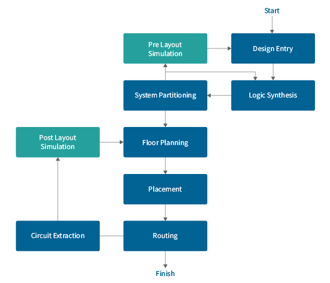
The process of designing an ASIC is done in stages. ASIC Design Flow is the name of this sequence of processes. The steps of the design flow are depicted in the flow chart below.
ASIC Physical Layout
Following the completion of the physical design, the layout must be thoroughly tested to guarantee proper electrical and logical performance. Some physical verification issues can be overlooked if their influence on chip yield is minimal. As a result, layout adjustments are normally done manually by skilled design engineers at this point.
Physical verification is broken down into the following steps: A. Design Rule Check (DRC) to ensure that the design has a high overall yield and dependability. B. Layout versus Schematic (LVS) tests to ensure the layout accurately depicts the circuit you want to build. C. Check the antenna to avoid gate oxide damage caused by charge collection owing to the antenna effect.
This flow will give a netlist that is ready for tape-out and may undergo some changes to meet
the timing constraints of engineering order change (ECO).

Prototype Tapeout:
The foundry receives the ASIC layout database for manufacturing. This is referred to as a “tape out.“ After 2 to 3 months, Faststream generally receives 3-12 wafers from the foundry holding the prototype ASIC design. To be tested against ATP, these wafers are split into dies and packaged for ATP testing. Every item in the ATP is examined, and any flaws or “bugs” are identified. If no defects are found, the design is immediately put into production. If flaws are found, they may be addressed by a specification and ATP update or the design may be adjusted to remedy the disparity, and a second-spin prototype tape out is performed after design and layout revisions. The work necessary for second-spin schematic design and layout is often much less than that required for first-spin schematic design and layout. Bugs can often be solved by changing just one mask layer, and a second-spin prototype fab can be significantly less expensive and faster than the first.
Production Mask set:
The prototype mask set can generate 6–12 wafers and can only be used once. A production mask set must be acquired if more ASICs are required. This mask set may be used to make wafers in lots of 25 endlessly. Following the fabrication of an approved prototype, the same layout database is utilized to create the production mask set.
Production Test Development:
A probe card is constructed, and test equipment is installed. Therefore, the die on the wafer can be examined on an automated wafer prober according to the production test plan, which is a subset of the ATP. A test program is created to put this production test strategy into action.